报告题目:Mapping Carrier Dynamics on Semiconductor Material Surfaces and at Interfaces using Laser Spectroscopy and 4D Electron Microscopy
报告人:Omar F. Mohammed,助理教授,阿卜杜拉国王科技大学
主持人: 梁文锡 教授
报告时间:2017年3月29日10:30-11:30 AM
地 点:武汉光电国家实验室(筹)A302
报告人简介:Dr. Mohammed is an Assistant Professor in the Division of Physical Sciences and Engineering. He is the principal investigator of ultrafast laser spectroscopy and four-dimensional electron imaging laboratory and he is affiliated with Solar and Photovoltaics Engineering Research Center at KAUST, and at present, his research activities are focused on the development of highly efficient solar cells with the aid of cutting-edge nanotechnology, laser spectroscopy, and ultrafast electron imaging. Prior to joining KAUST in December 2012, Dr. Mohammed was a senior research associate in Professor Ahmed Zewail’s group at Caltech, USA. While there, Dr. Mohammed joined the research group of Professor Zewail and worked on the development of new laser spectroscopic and time-resolved electron imaging techniques. Prior to his arrival in Pasadena, California, Dr. Mohammed spent more than a decade in Germany, Switzerland and Japan, embarking on the development of new laser spectroscopic techniques for direct observation of many chemical, physical and biological processes in real time. The accomplishments of Dr. Mohammed have resulted in more than 120 articles, invited talks and conference proceedings; and a large number of these papers are published in very high impact scientific journals including Science, Advanced Materials, Nano Letters, Advanced Energy Materials, Angewandte Chemie, PNAS, JACS, Chemical Communications, Advanced Functional Materials, Journal of Physical Chemistry Letters and Small.

报告摘要:
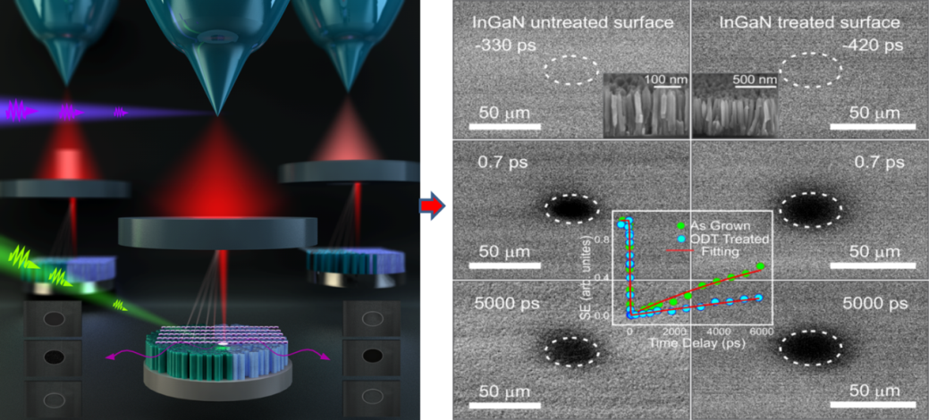
Interactions at material surfaces and interfaces have been among the most active areas of research in the last decade. This activity can be attributed to the important role that surface reactions play in a wide range of technological applications, including interfacial chemistry, Nanotechnology and photovoltaics. However, the ability to access carrier dynamics selectively on material surfaces with high spatial and temporal control in a photo-induced reaction is a particularly challenging task that can only be achieved by applying four-dimensional ultrafast electron microscopy (4D UEM). For this purpose, we established and developed the second generation of four-dimensional scanning ultrafast electron microscopy (4D S-UEM) at KAUST and demonstrate the ability to take time-resolved secondary electrons images (snapshots) of material surfaces with 650 fs and ~ 5 nm temporal and spatial resolutions, respectively. In this method, the surface of the photoactive materials is excited by a clocking optical pulse and the photo-induced changes will be imaged using a pulsed primary electron beam as a probe pulse, generating secondary electrons, which are emitted from the surface of the specimen in a manner that is sensitive to the local electron/hole density. This method provides direct and controllable dynamical information regarding surface dynamics. For instance, we clearly demonstrate how the surface morphology, grains, defects and nanostructured features can significantly impact the overall dynamical processes on the surface of photoactive-materials. Moreover, we show that the energy loss and carrier spreading on the surfaces of InGaN nanowires can be achieved now in real space. We have also mapped the charge-carrier recombination selectively on the surface of these nanowires before and after surface passivation with octadecylthiol (ODT). The time-resolved images (snapshots) clearly demonstrate that carrier recombination on the nanowires surface is significantly slowed after surface treatment, providing clear evidence of the minimization of the surface defects upon passivation, explaining clearly why the performance of optoelectronic device based on these materials is much better after surface passivation (Figure 1). In another interesting work describes a breakthrough in mapping charge carrier dynamics on the surface of quaternary copper indium gallium selenide (CIGSe) nanocrystals (commonly used in solar and optoelectronic devices) using S-UEM. The time-resolved images provided by S-UEM clearly demonstrate how surface treatment with high band gap materials such as ZnS can control the overall carrier relaxation process on the surfaces of these materials (Figure 2). More specifically, SE images at different time delays of treated nanocrystal surfaces clearly indicate that the carrier dynamics is slowed down by at least factor of two, indicating that the density of the trap states is significantly reduced after surface treatment with ZnS inorganic layer.

Figure 1: Schematic representation of our experimental setup for mapping InGaN NWs before and after surface treatment (left panel). Time-resolved SE di_erence images exhibiting the contrast evolution in InGaN nanowires before (left) and after (right) ODT passivation at selected time delays.

Figure 2: Representative TEM images of CIGS nanocrystals before and after ZnS surface treatment (left panel). Time-resolved SE di_erence images exhibiting the contrast evolution in CIGSe before and after ZnS shelling at selected time delays (right panel).