An international team of researchers is taking steps to bridge the gap between nanophotonics and nanomechanics by harnessing the induced near-field force within a nanocavity.
Yuchuan Jian at Fudan University and at Duke University in Durham, N.C., together with colleagues Junjun Xiao at Hong Kong University of Science and Technology and at Harbin Institute of Technology in Shenzhen and Jiping Huang at Fudan University, has designed the first powerful optical tweezer system that operates on the nanoscale.
In the device, a strong local field is generated by a nanocavity within a photonic crystal slab. This intense localized force can be used to manipulate, sort and select nearby complex dielectric nanorods.
“ For the first time, we have proposed the use of a remarkably localized nanocavity as a general light source,” Jian said. “ The photonic crystal cavity can exert an optical force on dielectric nanorods that have a high refractive index – much in the same way as a near-field optical tweezer.”

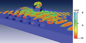
Shown is distribution of the normalized electromagnetic energy (U) in the coupled system. Here, k is the Boltzmann constant and T, the room temperature. An attractive optically induced potential ball is formed at the top part of the nanorod.

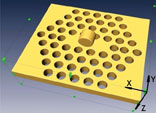
This schematic graph shows the system of a nanorod coupled with the cavity of a photonic crystal slab. Notice that the system axis Z is perpendicular to the slab (X-Y plane) in the figure. Images courtesy of Duke University.
Today’s optical tweezers use the concentrated gradient potential nature of a tightly focused laser beam to trap cells. However, manipulating objects on the nanoscale requires much stronger confinement of light, beyond the normal diffraction limit.
Jian and colleagues turned to photonic crystal nanocavities, which are ideal candidates for next-generation near-field optical tweezers because of their compact size and straightforward fabrication process. Jian said the devices can locally address individual nanorods, promising benefits to biosensing, cell/DNA isolation and molecule sieving applications.
“ Our device could be used in future on-chip integrated photonic circuits on the nanoscale,” he noted. “ Our specific goal is to show that a potential all-optical coupling operation using light can be achieved by the synthesized optomechanical potentials in this integrated system. We also want to demonstrate that the device can be applied in current semiconductor nanodevice fabrication processes.”
In the computational experiment, described in the Journal of Physical Chemistry C on Sept. 3, 2009, a dielectric nanorod is placed above a high-Q photonic crystal cavity. An optical-dipole force field surrounds the cavity and interacts with the nearby nanorod. In turn, the nanorod creates small perturbations within the high-Q cavity, which affects the system’s behavior and stability.
“ An optical force is exerted on the nanorod, which pushes or pulls it to an equilibrium position, thanks to the evolving attractive/repulsive interaction between the nanorod and cavity,” Jian said. “ What’s more, this optical force or light source is tunable through spontaneous emission within the nanocavity.”
The Fudan-Duke group recognizes that much work still must be done to bridge the gap between current fundamental research and future industrial applications. The next step is to extend the calculations to investigate an array of nanocavities to see whether both parallel and large-scale manipulation is possible. Another avenue of research planned by the team is to shift the working frequency to determine whether broadband operation is possible.
(责任编辑:董静)