REVIEW ARTICLE
Recent progress of semiconductor optoelectronic fibers
DOI: 10.1007/s12200-021-1226-0
Hei Chit Leo TSUI, Noel HEALY
Abstract:
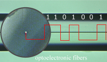
Semiconductor optoelectronic fiber technology has seen rapid development in recent years thanks to advancements in fabrication and post-processing techniques. Integrating the optical and electronic functionality of semiconductor materials into a fiber geometry has opened up many possibilities, such as in-fiber frequency generation, signal modulation, photodetection, and solar energy harvesting. This review provides an overview of the state-of-the-art in semiconductor optoelectronic fibers, including fabrication and post-processing methods, materials and their optical properties. The applications in nonlinear optics, optical-electrical conversion, lasers and multimaterial functional fibers will also be highlighted.
半导体光电子光纤技术近年来由于制造和后处理技术的进步而得到了迅速发展。将半导体材料的光学和电子功能集成到光纤几何结构中开辟了许多可能性,例如光纤中的频率产生、信号调制、光电探测和太阳能收集。本文综述了半导体光电子光纤的发展现状,包括半导体光电子光纤的制备和后处理方法、材料及其光学性能,并讨论在非线性光学、光电转换、激光器和多材料功能光纤等方面的应用。
Cite this article: Hei Chit Leo TSUI, Noel HEALY. Recent progress of semiconductor optoelectronic fibers[J]. Frontiers of Optoelectronics, 2021, 14(4): 383‒398
RESEARCH ARTICLE
Optical trapping using transverse electromagnetic (TEM)-like mode in a coaxial nanowaveguide
DOI: 10.1007/s12200-021-1134-3
Yuanhao LOU, Xiongjie NING, Bei WU, Yuanjie PANG
Abstract:
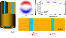
Optical traps have emerged as powerful tools for immobilizing and manipulating small particles in three dimensions. Fiber-based optical traps (FOTs) significantly simplify optical setup by creating trapping centers with single or multiple pieces of optical fibers. In addition, they inherit the flexibility and robustness of fiber-optic systems. However, trapping 10-nm-diameter nanoparticles (NPs) using FOTs remains challenging. In this study, we model a coaxial waveguide that works in the optical regime and supports a transverse electromagnetic (TEM)-like mode for NP trapping. Single NPs at waveguide front-end break the symmetry of TEM-like guided mode and lead to high transmission efficiency at far-field, thereby strongly altering light momentum and inducing a large-scale back-action on the particle. We demonstrate, via finite-difference time-domain (FDTD) simulations, that this FOT allows for trapping single 10-nm-diameter NPs at low power.
光阱已经成为固定和操纵三维小粒子的有力工具。基于光纤的光阱(FOT)通过使用单个或多个光纤创建陷阱中心,大大简化了光学装置。此外,它们继承了光纤系统的灵活性和鲁棒性。然而,使用FOTs捕获直径为10nm的纳米颗粒(NPs)仍然具有挑战性。在这项研究中,我们建立了一个工作在光频段、支持类横向电磁(TEM)模式的同轴波导模型,用于NP捕获。波导前端的单个NPs破坏了类TEM导模的对称性,并导致远场的高传输效率,从而强烈改变了光动量,并对粒子产生了大的反向作用。我们通过时域有限差分(FDTD)模拟,证明了该FOT可以在低功率下捕获单个直径为10 nm的NPs。
Cite this article: Yuanhao LOU, Xiongjie NING, Bei WU, Yuanjie PANG. Optical trapping using transverse electromagnetic (TEM)-like mode in a coaxial nanowaveguide[J]. Frontiers of Optoelectronics, 2021, 14(4): 399‒406
Design of hollow core step-index antiresonant fiber with stepped refractive indices cladding
DOI: 10.1007/s12200-020-1109-9
Botao DENG, Chaotan SIMA, Hongyu TAN, Xiaohang ZHANG, Zhenggang LIAN, Guoqun CHEN, Qianqing YU, Jianghe XU, Deming LIU
Abstract:
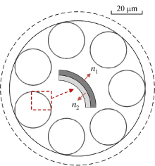
With the benefits of low latency, wide transmission bandwidth, and large mode field area, hollow-core antiresonant fiber (HC-ARF) has been a research hotspot in the past decade. In this paper, a hollow core step-index antiresonant fiber (HC-SARF), with stepped refractive indices cladding, is proposed and numerically demonstrated with the benefits of loss reduction and bending improvement. Glass-based capillaries with both high (n = 1.45) and low (as low as n = 1.36) refractive indices layers are introduced and formatted in the cladding air holes. Using the finite element method to perform numerical analysis of the designed fiber, results show that at the laser wavelengths of 980 and 1064 nm, the confinement loss is favorably reduced by about 6 dB/km compared with the conventional uniform cladding HC-ARF. The bending loss, around 15 cm bending radius of this fiber, is also reduced by 2 dB/km. The cladding air hole radius in this fiber is further investigated to optimize the confinement loss and the mode field diameter with single-mode transmission behavior. This proposed HC-SARF has great potential in optical fiber transmission and high energy delivery.
空心抗共振光纤(HC-ARF)以其低延迟、宽传输带宽、大模场面积等优点成为近十年来的研究热点。本文提出了一种具有阶跃折射率包层的空芯阶跃折射率抗共振光纤(HC-SARF),并用数值方法证明了其具有降低损耗和改善弯曲的优点。该光纤在包层空气孔中引入了具有高(n=1.45)、低(低至n=1.36)折射率层的玻璃毛细管。利用有限元方法对设计的光纤进行了数值分析,结果表明,在980和1064nm的激光波长下,与传统的均匀包层HC-ARF相比,模场限制损耗降低了约6dB/km。这种光纤的弯曲半径约为15 cm,弯曲损耗也降低了2 dB/km。进一步研究了该光纤包层空气孔半径,以优化模场限制损耗和单模传输模式下的模场直径。这种HC-SARF在光纤传输和高能光场传送方面具有巨大的潜力。
Cite this article: Botao DENG, Chaotan SIMA, Hongyu TAN, Xiaohang ZHANG, Zhenggang LIAN, Guoqun CHEN, Qianqing YU, Jianghe XU, Deming LIU. Design of hollow core step-index antiresonant fiber with stepped refractive indices cladding[J]. Frontiers of Optoelectronics, 2021, 14(4): 407‒413
Toward coherent O-band data center interconnects
DOI: 10.1007/s12200-021-1242-0
Pascal M. SEILER, Galina GEORGIEVA, Georg WINZER, Anna PECZEK, Karsten VOIGT, Stefan LISCHKE, Adel FATEMI, Lars ZIMMERMANN
Abstract:
Upcoming generations of coherent intra/inter data center interconnects currently lack a clear path toward a reduction of cost and power consumption, which are the driving factors for these data links. In this work, the trade-offs associated with a transition from coherent C-band to O-band silicon photonics are addressed and evaluated. The discussion includes the fundamental components of coherent data links, namely the optical components, fiber link and transceivers. As a major component of these links, a monolithic silicon photonic BiCMOS O-band coherent receiver is evaluated for its potential performance and compared to an analogous C-band device.
新一代数据中心内部/之间的相干互连目前缺乏降低成本和功耗的明确途径,而成本和功耗是这些数据链路发展的驱动因素。在这项工作中,我们讨论和评估了从相干C波段转变到O波段时硅光子学中需要权衡的问题。讨论内容包括相干数据链路的基本组成部分,即光学元件、光纤链路和收发器。对这些链路的主要组成部分——单片硅光子BiCMOS O波段相干接收机的性能进行了评估,并与类似的C波段器件进行了比较。
Cite this article: Pascal M. SEILER, Galina GEORGIEVA, Georg WINZER, Anna PECZEK, Karsten VOIGT, Stefan LISCHKE, Adel FATEMI, Lars ZIMMERMANN. Toward coherent O-band data center interconnects[J]. Frontiers of Optoelectronics, 2021, 14(4): 414‒425

Optical generation of UWB pulses utilizing Fano resonance modulation
DOI: 10.1007/s12200-020-1010-6
Zhe XU, Yanyang ZHOU, Shuhuang CHEN, Liangjun LU, Gangqiang ZHOU, Jianping CHEN, Linjie ZHOU
Abstract:
In this paper, we reported an integrated method to generate ultra-wideband (UWB) pulses of different orders based on a reconfigurable silicon micro-ring resonator-coupled Mach–Zehnder interferometer. Under proper operating conditions, the device can produce Fano resonances with a peak-to-valley extinction ratio of above 20 dB. UWB monocycle and doublet signals with picosecond pulse widths are produced when the micro-ring resonator is modulated by square and Gaussian electrical pulses, respectively. With our Fano resonance modulator on silicon photonics, it is promising to foresee versatile on-chip microwave signal generation.
本文报道了一种基于可重构微环谐振器耦合马赫-曾德尔干涉仪产生不同阶次超宽带(UWB)脉冲的硅基集成器件。在适当的工作条件下,该器件可以产生峰谷消光比大于20dB的Fano共振。当微环谐振器分别被方形和高斯电脉冲调制时,产生了皮秒脉冲宽度的超宽带monocycle和doublet信号。利用我们的硅光子学Fano共振调制器,有望实现多功能片上微波信号产生。
Cite this article: Zhe XU, Yanyang ZHOU, Shuhuang CHEN, Liangjun LU, Gangqiang ZHOU, Jianping CHEN, Linjie ZHOU. Optical generation of UWB pulses utilizing Fano resonance modulation[J]. Frontiers of Optoelectronics, 2021, 14(4): 426‒437

Singular PT-symmetry broken point with infinite transmittance and reflectance----a classical analytical demonstration
DOI: 10.1007/s12200-020-0969-3
Yingxin JIANG
Abstract:
To demonstrate the existence of singular parity-time symmetry (PT-symmetry) broken point in optics system, we designed a one-dimensional PT symmetric structure including N unit-cell with loss and gain materials in half. We performed an analytical deduction to obtain the transmittance and reflectance of the structure basing on Maxwell’s equations. We found that with the exact structure unit-cell number and the imaginary part of refraction index, the transmittance and reflectance are both close to infinite. Such strict condition is called the singular point in this study. At the singular point position, both the transmission and reflection are direction-independent. Away from the singular point, the transmittance and reflectance become finite. In light of classical wave optics, the single unit and total structure both become the resonance units. The infinite transmittance and reflectance result from the resonance matching of single unit and total structure. In light of quantum theory, the singular point corresponds to the single eigenvalue of electromagnetic scattering matrix. The infinite transmittance and reflectance mean a huge energy transformation from pumping source to light waves. Numerical calculation and software simulation both demonstrate the result.
为了证明光学系统中宇称时间对称(PT对称)破缺奇点的存在,我们设计了一种一维PT对称结构,其中包括N个单元,每个单元中损耗和增益材料各占一半。基于麦克斯韦方程,我们推导了该结构的透射率和反射率。我们发现,在结构单元数和折射率虚部取某一确定值的情况下,透射率和反射率都接近无穷大。在本研究中这一严格条件称为奇点。在奇点位置,透射和反射都是方向无关的。离开奇点,透射率和反射率变为有限。根据经典波动光学,单个单元和整个结构都可以看做共振单元。无限的透射率和反射率是单个单元和整体结构共振匹配的结果。根据量子理论,奇点对应于电磁散射矩阵的单一特征值。无限的透射率和反射率意味着从泵浦源到光波巨大的能量转换。数值计算和软件仿真都证明了这一结果。
Cite this article: Yingxin JIANG. Singular PT-symmetry broken point with infinite transmittance and reflectance----a classical analytical demonstration[J]. Frontiers of Optoelectronics, 2021, 14(4): 438‒444

Interface phonon polariton coupling to enhance graphene absorption
DOI: 10.1007/s12200-019-0957-7
Zhenyao CHEN, Junjie MEI, Ye ZHANG, Jishu TAN, Qing XIONG, Changhong CHEN
Abstract:
Here we present a graphene photodetector of which the graphene and structural system infrared absorptions are enhanced by interface phonon polariton (IPhP) coupling. IPhPs are supported at the SiC/AlN interface of device structure and used to excite interband transitions of the intrinsic graphene under gated-field tuning. The simulation results show that at normal incidence the absorbance of graphene or system reaches up to 43% or closes to unity in a mid-infrared frequency range. In addition, we found the peak-absorption frequency is mainly decided by the AlN thickness, and it has a red-shift as the thickness decreases. This structure has great application potential in graphene infrared detection technology.
我们提出了一种石墨烯光电探测器,器件整体及石墨烯中的红外吸收通过界面声子极化激元(IPhP)耦合得到增强。该器件的SiC/AlN界面上支持IPhP,通过电场调谐可激发本征石墨烯的带间跃迁。模拟结果表明,在正入射下,石墨烯的吸收率在中红外频率范围内达到43%,器件整体的吸收率则接近1。此外,我们还发现,峰值吸收频率主要由AlN厚度决定,并且随着厚度的减小,峰值吸收频率会发生红移。这种结构在石墨烯红外探测技术中具有很大的应用潜力。
Cite this article: Zhenyao CHEN, Junjie MEI, Ye ZHANG, Jishu TAN, Qing XIONG, Changhong CHEN. Interface phonon polariton coupling to enhance graphene absorption[J]. Frontiers of Optoelectronics, 2021, 14(4): 445‒449
REVIEW ARTICLE
Recent progress in the research on using CuSbS2 and its derivative CuPbSbS3 as absorbers in case of photovoltaic devices
DOI: 10.1007/s12200-020-1024-0
Muyi ZHANG, Chong WANG, Chao CHEN, Jiang TANG
Abstract:
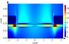
Thin-film solar cells show considerable application potential as alternative photovoltaic technologies. Cuprous antimony chalcogen materials and their derivatives, represented as CuSbS2 and CuPbSbS3, respectively, exhibit the advantages of low cost, massive elemental abundance, stability, and good photoelectric properties, including a suitable bandgap and large optical absorption coefficient. These advantages demonstrate that they can be used as light absorbers in photovoltaic applications. In this study, we review the major properties, fabrication methods, and recent progress of the performance of the devices containing CuSbS2 and CuPbSbS3. Furthermore, the limitations and future development prospects with respect to the CuSbS2 and CuPbSbS3 solar cells are discussed.
薄膜太阳能电池作为一种备选的光伏技术显示出巨大的应用潜力。分别以CuSbS2和CuPbSbS3为代表的亚铜锑硫系材料及其衍生物,不仅具有成本低、元素丰度大、稳定性好等优点,还具有好的光电性能,包括合适的带隙和较大的光吸收系数。这些优点表明它们可以用作光伏应用中的光吸收器。在这项研究中,我们回顾了含有CuSbS2和CuPbSbS3的器件的主要特性、制备方法和性能的最新进展。此外,还讨论了CuPbS2和CuPbSbS3太阳能电池的局限性和未来发展前景。
Cite this article: Muyi ZHANG, Chong WANG, Chao CHEN, Jiang TANG. Recent progress in the research on using CuSbS2 and its derivative CuPbSbS3 as absorbers in case of photovoltaic devices[J]. Frontiers of Optoelectronics, 2021, 14(4): 450‒458

Self-trapped exciton emission in inorganic copper(I) metal halides
DOI: 10.1007/s12200-021-1133-4
Boyu ZHANG, Xian WU, Shuxing ZHOU, Guijie LIANG, Qingsong HU
Abstract:
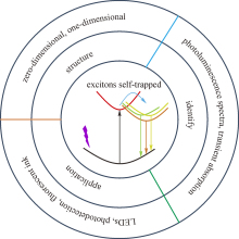
The broad emission and high photoluminescence quantum yield of self-trapped exciton (STE) radiative recombination emitters make them an ideal solution for single-substrate, white, solid-state lighting sources. Unlike impurities and defects in semiconductors, the formation of STEs requires a lattice distortion, along with strong electron–phonon coupling, in low electron-dimensional materials. The photoluminescence of inorganic copper(I) metal halides with low electron-dimensionality has been found to be the result of STEs. These materials were of significant interest because of their lead-free, all-inorganic structures, and high luminous efficiencies. In this paper, we summarize the luminescence characteristics of zero- and one-dimensional inorganic copper(I) metal halides with STEs to provide an overview of future research opportunities.
自陷激子(STE)辐射复合发射体具有发射谱宽、光致发光量子产率高的优点,是单衬底白光固态光源的理想解决方案。与半导体中的杂质和缺陷不同,在低维电子材料中,STE的形成需要晶格畸变以及强烈的电子-声子耦合。低维无机铜(I)金属卤化物的光致发光是STEs的结果。这些材料因其无铅、全无机结构和高发光效率而备受关注。在本文中,我们总结了具有自陷激子的零维和一维无机铜(I)金属卤化物的发光特性,以考察其未来可能的研究方向。
Cite this article: Boyu ZHANG, Xian WU, Shuxing ZHOU, Guijie LIANG, Qingsong HU. Self-trapped exciton emission in inorganic copper(I) metal halides[J]. Frontiers of Optoelectronics, 2021, 14(4): 459‒472
RESEARCH ARTICLE
Oxide perovskite Ba2AgIO6 wafers for X-ray detection
DOI: 10.1007/s12200-021-1236-y
Longbo YANG, Jincong PANG, Zhifang TAN, Qi XIAO, Tong JIN, Jiajun LUO, Guangda NIU, Jiang TANG
Abstract:
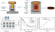
X-ray detection is of great significance in biomedical, nondestructive, and scientific research. Lead halide perovskites have recently emerged as one of the most promising materials for direct X-ray detection. However, the lead toxicity remains a worrisome concern for further commercial application. Great efforts have been made to search for lead-free perovskites with similar optoelectronic properties. Here, we present a lead-free oxide double perovskite material Ba2AgIO6 for X-ray detection. The lead-free, all-inorganic nature, as well as the high density of Ba2AgIO6, promises excellent prospects in X-ray applications. By employing the hydrothermal method, we successfully synthesized highly crystalline Ba2AgIO6 powder with pure phase. Furthermore, we prepared Ba2AgIO6 wafers through isostatic pressure and built X-ray detectors with Au/Ba2AgIO6 wafer/Au photoconductive structure. The as-prepared X-ray detectors showed a sensitivity of 18.9 μC/(Gyair·cm2) at 5 V/mm, similar to commercial α-Se detectors showcasing their advantages for X-ray detection.
X射线探测在生物医学、无损检测和科学研究中具有重要意义。卤化铅钙钛矿是近年来出现的最有前途的一种直接探测X射线的材料。然而,铅毒性仍然是其进一步商业应用的一个令人担忧的问题。人们一直在努力寻找具有类似光电性质的无铅钙钛矿。在此,我们提出了一种用于X射线探测的无铅氧化物双钙钛矿材料Ba2AgIO6。Ba2AgIO6所具有的无铅、全无机性质以及高密度,使其在X射线应用中前景广阔。我们采用水热法成功合成了高结晶度的纯相Ba2AgIO6粉末,采用等静压法制备了Ba2AgIO6晶片,并制备了具有Au/ Ba2AgIO6晶片/Au光电导结构的X射线探测器。所制备的X射线探测器在5V/mm偏置下灵敏度为18.9μC/(Gyair·cm2),类似于商用α-Se探测器,显示了其在X射线探测方面的优势。
Cite this article: Longbo YANG, Jincong PANG, Zhifang TAN, Qi XIAO, Tong JIN, Jiajun LUO, Guangda NIU, Jiang TANG. Oxide perovskite Ba2AgIO6 wafers for X-ray detection[J]. Frontiers of Optoelectronics, 2021, 14(4): 473‒481
Rapid thermal evaporation for cadmium selenide thin-film solar cells
DOI: 10.1007/s12200-021-1217-1
Kanghua LI, Xuetian LIN, Boxiang SONG, Rokas KONDROTAS, Chong WANG, Yue LU, Xuke YANG, Chao CHEN, Jiang TANG
Abstract:
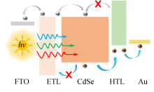
Cadmium selenide (CdSe) belongs to the binary II-VI group semiconductor with a direct bandgap of ~1.7 eV. The suitable bandgap, high stability, and low manufacturing cost make CdSe an extraordinary candidate as the top cell material in silicon-based tandem solar cells. However, only a few studies have focused on CdSe thin-film solar cells in the past decades. With the advantages of a high deposition rate (~2 µm/min) and high uniformity, rapid thermal evaporation (RTE) was used to maximize the use efficiency of CdSe source material. A stable and pure hexagonal phase CdSe thin film with a large grain size was achieved. The CdSe film demonstrated a 1.72 eV bandgap, narrow photoluminescence peak, and fast photoresponse. With the optimal device structure and film thickness, we finally achieved a preliminary efficiency of 1.88% for CdSe thin-film solar cells, suggesting the applicability of CdSe thin-film solar cells.
硒化镉(CdSe)属于二元II-VI族半导体,直接带隙约为1.7ev。合适的带隙、高稳定性和低制造成本使CdSe成为硅基串联太阳能电池的顶级电池材料。然而,在过去几十年中,只有少数研究集中在CdSe薄膜太阳能电池上。由于具有沉积速率高(~2µm/min)和均匀性好的优势,快速热蒸发(RTE)被用于最大限度地提高CdSe源材料的使用效率。本工作中我们制备了稳定的大晶粒纯六方相CdSe薄膜。CdSe薄膜具有1.72ev的带隙、窄的光致发光峰和快速的光响应。通过优化器件结构和薄膜厚度,CdSe薄膜太阳能电池的初步效率达到1.88%,表明了CdSe薄膜太阳能电池的适用性。
Cite this article: Kanghua LI, Xuetian LIN, Boxiang SONG, Rokas KONDROTAS, Chong WANG, Yue LU, Xuke YANG, Chao CHEN, Jiang TANG. Rapid thermal evaporation for cadmium selenide thin-film solar cells[J]. Frontiers of Optoelectronics, 2021, 14(4): 482‒490
Improved stability of blue TADF organic electroluminescent diodes via OXD-7 based mixed host
DOI: 10.1007/s12200-020-1069-0
Weiguang LI, Jie TANG, Yanqiong ZHENG, Junbiao PENG, Jianhua ZHANG, Bin WEI, Xifeng LI
Abstract:
Thermally activated delayed fluorescence (TADF) organic light-emitting diodes (OLEDs) have been demonstrated in applications such as displays and solid-state lightings. However, weak stability and inefficient emission of blue TADF OLEDs are two key bottlenecks limiting the development of solution processable displays and white light sources. This work presents a solution-processed OLED using a blue-emitting TADF small molecule bis[4-(9,9-dimethyl-9,10-dihydroacridine)phenyl]sulfone (DMAC-DPS) as an emitter. We comparatively investigated the effects of single host poly(N-vinylcarbazole) (PVK) and a co-host of 60% PVK and 30% 2,2′-(1,3-phenylene)-bis[5-(4-tert-butylphenyl)-1,3,4-oxadiazole] (OXD-7) on the device performance (the last 10% is emitter DMAC-DPS). The co-host device shows lower turn-on voltage, similar maximum luminance, and much slower external quantum efficiency (EQE) roll-off. In other words, device stability improved by doping OXD-7 into PVK, and the device impedance simultaneously and significantly reduced from 8.6 × 10³ to 4.2 × 10³ W at 1000 Hz. Finally, the electroluminescent stability of the co-host device was significantly enhanced by adjusting the annealing temperature.
热激活延迟荧光(TADF)有机发光二极管(OLED)在显示器和固态照明等方面的应用已得到证实。然而,蓝光TADF OLED稳定性差和发射效率低的问题仍然是限制湿法制备显示器和白光源发展的两个关键瓶颈。本工作提出了一种使用蓝光发射TADF小分子DMAC-DPS作为发射体的湿法制备OLED。我们比较研究了采用PVK单基质和60%PVK、30%OXD-7共基质对器件性能的影响(最后10%为发射体DMAC-DPS)。共基质器件显示出较低的开启电压、类似的最大亮度和较慢的外部量子效率(EQE)衰减。换句话说,在PVK中掺杂OXD-7可以提高器件的稳定性,同时在1000Hz处器件的阻抗也从8.6×10³显著降低到4.2×10³。最后,通过调整退火温度,可显著提高共基质器件的电致发光稳定性。
Cite this article: Weiguang LI, Jie TANG, Yanqiong ZHENG, Junbiao PENG, Jianhua ZHANG, Bin WEI, Xifeng LI. Improved stability of blue TADF organic electroluminescent diodes via OXD-7 based mixed host[J]. Frontiers of Optoelectronics, 2021, 14(4): 491‒498

Light-emission organic solar cells with MoO3:Al interfacial layer–preparation and characterizations
DOI: 10.1007/s12200-020-1103-2
Xinran LI, Yanhui LOU, Zhaokui WANG
Abstract:
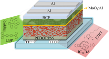
A light-emitting organic solar cell (LE-OSC) with electroluminescence (EL) and photovoltaic (PV) properties is successfully fabricated by connecting the EL and PV units using a MoO3:Al co-evaporation interfacial layer, which has suitable work function and good transmittance. PV and EL units are fabricated based on poly(3-hexylthiophene) (P3HT)-indene-C60 bisadduct (IC60BA) blends, and 4,4′-bis (N-carbazolyl) biphenyl-fac-tris (2-phenylpyridine) iridium (Ir(ppy)3), respectively. The work function and the transmittance of the MoO3:Al co-evaporation are measured and adjusted by the ultraviolet photoelectron spectroscopy and the optical spectrophotometer to obtain the better bi-functional device performance. The forward- and reverse-biased current density-voltage characteristics in dark and under illumination are evaluated to better understand the operational mechanism of the LE-OSCs. A maximum luminance of 1550 cd/m2 under forward bias and a power conversion efficiency of 0.24% under illumination (100 mW/cm2) are achieved in optimized LE-OSCs. The proposed device structure is expected to provide valuable information in the film conditions for understanding the polymer blends internal conditions and meliorating the film qualities.
我们通过采用具有合适功函数和良好透射率MoO3:Al共蒸发界面层将电致发光(EL)和光伏(PV)单元连接起来,成功制备了同时具有EL和PV特性的发光有机太阳能电池(LE-OSC)。PV和EL单元分别基于P3HT:IC60BA和(CBP:Ir(ppy)3 制备。利用紫外光电子能谱仪和光学分光光度计对MoO3:Al共蒸发的功函数和透射率进行了测量和调整,以获得更好的双功能器件性能。为了更好地理解LE-OSC的工作机理,我们评估了在黑暗和光照条件下正向和反向偏置时的电流密度-电压特性。优化的LE-OSC在正向偏压下的最大亮度为1550 cd/m2,在100 mW/cm2光下功率转换效率为0.24%。所提出的器件结构有望为认识聚合物共混物的内部条件和改善薄膜质量提供有价值的有关薄膜条件的信息。
Cite this article: Xinran LI, Yanhui LOU, Zhaokui WANG. Light-emission organic solar cells with MoO3:Al interfacial layer–preparation and characterizations[J]. Frontiers of Optoelectronics, 2021, 14(4): 499‒506
Growth of InGaN-based blue-LED on AlN/sapphire sputtered with different oxygen flow rate
DOI: 10.1007/s12200-021-1216-2
Jiahui HU, Feng WU, Jiangnan DAI, Changqing CHEN
Abstract:
Indium Gallium Nitride based blue light-emitting diodes (LEDs) suffer from insufficient crystal quality and serious efficiency droop in large forward current. In this paper, the InGaN-based blue LEDs are grown on sputtered aluminum nitride (AlN) films to improve the device light power and weaken the efficiency droop. The effects of oxygen flow rate on the sputtering of AlN films on sapphire and device performance of blue LEDs are studied in detail. The mechanism of external quantum efficiency improvement is related to the change of V-pits density in multiple quantum wells. The external quantum efficiency of 66% and 3-V operating voltage are measured at a 40-mA forward current of with the optimal oxygen flow rate of 4 SCCM.
铟镓氮(InGaN)基蓝光发光二极管(LED)在大的正向电流下存在晶体质量不足和严重的效率下降问题。本文在溅射氮化铝(AlN)薄膜上生长了InGaN基蓝光LED,以提高器件的光功率并缓解效率下降的问题。我们详细研究了氧流量对蓝宝石上AlN薄膜溅射和蓝光LED器件性能的影响,结果表明外量子效率的提高机制与多量子阱中V型坑密度的变化有关。采用4sccm的最佳氧流量,在40mA正向电流下,测得外量子效率为66%,工作电压为3V。
Cite this article: Jiahui HU, Feng WU, Jiangnan DAI, Changqing CHEN. Growth of InGaN-based blue-LED on AlN/sapphire sputtered with different oxygen flow rate[J]. Frontiers of Optoelectronics, 2021, 14(4): 507‒512

A QoT prediction technique based on machine learning and NLSE for QoS and new lightpaths in optical communication networks
DOI: 10.1007/s12200-020-1079-y
Yongfeng FU, Jing CHEN, Weiming WU, Yu HUANG, Jie HONG, Long CHEN, Zhongbin LI
Abstract:
In this paper, we proposed a quality of transmission (QoT) prediction technique for the quality of service (QoS) link setup based on machine learning classifiers, with synthetic data generated using the transmission equations instead of the Gaussian noise (GN) model. The proposed technique uses some link and signal characteristics as input features. The bit error rate (BER) of the signals was compared with the forward error correction threshold BER, and the comparison results were employed as labels. The transmission equations approach is a better alternative to the GN model (or other similar margin-based models) in the absence of real data (i.e., at the deployment stage of a network) or the case that real data are scarce (i.e., for enriching the dataset/reducing probing lightpaths); furthermore, the three classifiers trained using the data of the transmission equations are more reliable and practical than those trained using the data of the GN model. Meanwhile, we noted that the priority of the three classifiers should be support vector machine (SVM)>K nearest neighbor (KNN)>logistic regression (LR) as shown in the results obtained by the transmission equations, instead of SVM>LR>KNN as in the results of the GN model.
在本文中,我们提出了一种基于机器学习分类器的服务质量(QoS)链路的传输质量(QoT)预测技术,其中采用了传输方程而不是高斯噪声(GN)模型来生成合成数据。该技术采用一些链路和信号特性作为输入特征。将信号的误码率(BER)与前向纠错阈值BER进行比较,并将比较结果作为标签。在缺乏真实数据(即,在网络部署阶段)或真实数据稀缺(即,用于丰富数据集/减少探测光路)的情况下,传输方程方法是比GN模型(或其他类似基于裕度的模型)更好的替代方法;此外,使用传输方程数据训练的三个分类器比使用GN模型数据训练的分类器更可靠和实用。同时我们注意到:传输方程得到的结果显示三个分类器的优先级应该是支持向量机(SVM)>K最近邻(KNN)>逻辑回归(LR),而不是GN模型结果中给出的SVM>LR>KNN。
Cite this article: Yongfeng FU, Jing CHEN, Weiming WU, Yu HUANG, Jie HONG, Long CHEN, Zhongbin LI. A QoT prediction technique based on machine learning and NLSE for QoS and new lightpaths in optical communication networks[J]. Frontiers of Optoelectronics, 2021, 14(4): 513‒521

Drilling high aspect ratio holes by femtosecond laser filament with aberrations
DOI: 10.1007/s12200-021-1214-4
Manshi WANG, Zhiqiang YU, Nan ZHANG, Weiwei LIU
Abstract:
A near-infrared femtosecond laser is focused by a 100 mm-focal-length plano-convex lens to form a laser filament, which is employed to drill holes on copper targets. By shifting or rotating the focusing lens, additional aberration is imposed on the focused laser beam, and significant influence is produced on the aspect ratio and cross-sectional shape of the micro-holes. Experimental results show that when proper aberration is introduced, the copper plate with a thickness of 3 mm can be drilled through with an aspect ratio of 30, while no through-holes can be drilled on 3-mm-thickness copper plates by femtosecond laser with minimized aberration. In addition, when femtosecond laser filament with large astigmatism is used, micro-holes that had a length to width ratio up to 3.3 on the cross-section are obtained. Therefore, the method proposed here can be used to fabricate long oval holes with high aspect ratios.
本工作中,近红外飞秒激光被一个焦距100毫米的平凸透镜聚焦,形成一个激光灯丝,用于在铜靶上钻孔。通过移动或旋转聚焦透镜,可对聚焦激光束施加额外的像差,从而对微孔的宽高比和截面形状产生显著影响。实验结果表明,当引入适当的像差时,3mm厚的铜板可以被钻穿形成宽高比为30的通孔,而在最小像差情况下飞秒激光不能在3mm厚的铜板上形成通孔。此外,当使用具有大像散的飞秒激光灯丝时,可获得横截面上长宽比高达3.3的微孔。因此,本文提出的方法可用于制作大宽高比的长椭圆孔。
Cite this article: Manshi WANG, Zhiqiang YU, Nan ZHANG, Weiwei LIU. Drilling high aspect ratio holes by femtosecond laser filament with aberrations[J]. Frontiers of Optoelectronics, 2021, 14(4): 522‒528

Improved phase retrieval in holographic data storage based on a designed iterative embedded data
DOI: 10.1007/s12200-021-1218-0
Changyu YU, Suping WANG, Ruixian CHEN, Jianying HAO, Qijing ZHENG, Jinyu WANG, Xianying QIU, Kun WANG, Dakui LIN, Yi YANG, Hui LI, Xiao LIN, Xiaodi TAN
Abstract:
Embedded data are used to retrieve phases quicker with high accuracy in phase-modulated holographic data storage (HDS). We propose a method to design an embedded data distribution using iterations to enhance the intensity of the high-frequency signal in the Fourier spectrum. The proposed method increases the anti-noise performance and signal-to-noise ratio (SNR) of the Fourier spectrum distribution, realizing a more efficient phase retrieval. Experiments indicate that the bit error rate (BER) of this method can be reduced by a factor of one after 10 iterations.
在相位调制全息数据存储(HDS)中,嵌入数据用于快速、高精度地恢复相位。我们提出了一种使用迭代来设计嵌入式数据分布的方法,以增强傅里叶频谱中高频信号的强度。该方法提高了傅里叶谱分布的抗噪声性能和信噪比,实现了更高效的相位恢复。实验表明,该方法经过10次迭代后,误码率可以降低1倍。
Cite this article: Changyu YU, Suping WANG, Ruixian CHEN, Jianying HAO, Qijing ZHENG, Jinyu WANG, Xianying QIU, Kun WANG, Dakui LIN, Yi YANG, Hui LI, Xiao LIN, Xiaodi TAN. Improved phase retrieval in holographic data storage based on a designed iterative embedded data[J]. Frontiers of Optoelectronics, 2021, 14(4): 529‒539